Overview
In this ongoing project, I am bridging the gap between theoretical knowledge and practical application by moving beyond textbooks into hands-on circuit design and layout work. Using Analog Integrated Circuit Design by Tony C. Carusone, David A. Johns and Kenneth W. Martin as a source of practice problems, I work through end-of-chapter exercises to design circuits, simulate them in LTSpice, and create layouts in KLayout. This process not only strengthens my technical skills in simulation and layout design but also supports my transition from student to professional in the field of semiconductor design.
Initial Circuits
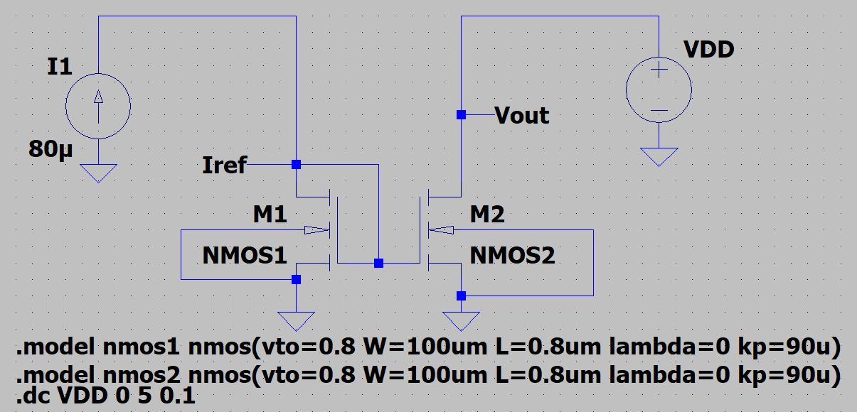
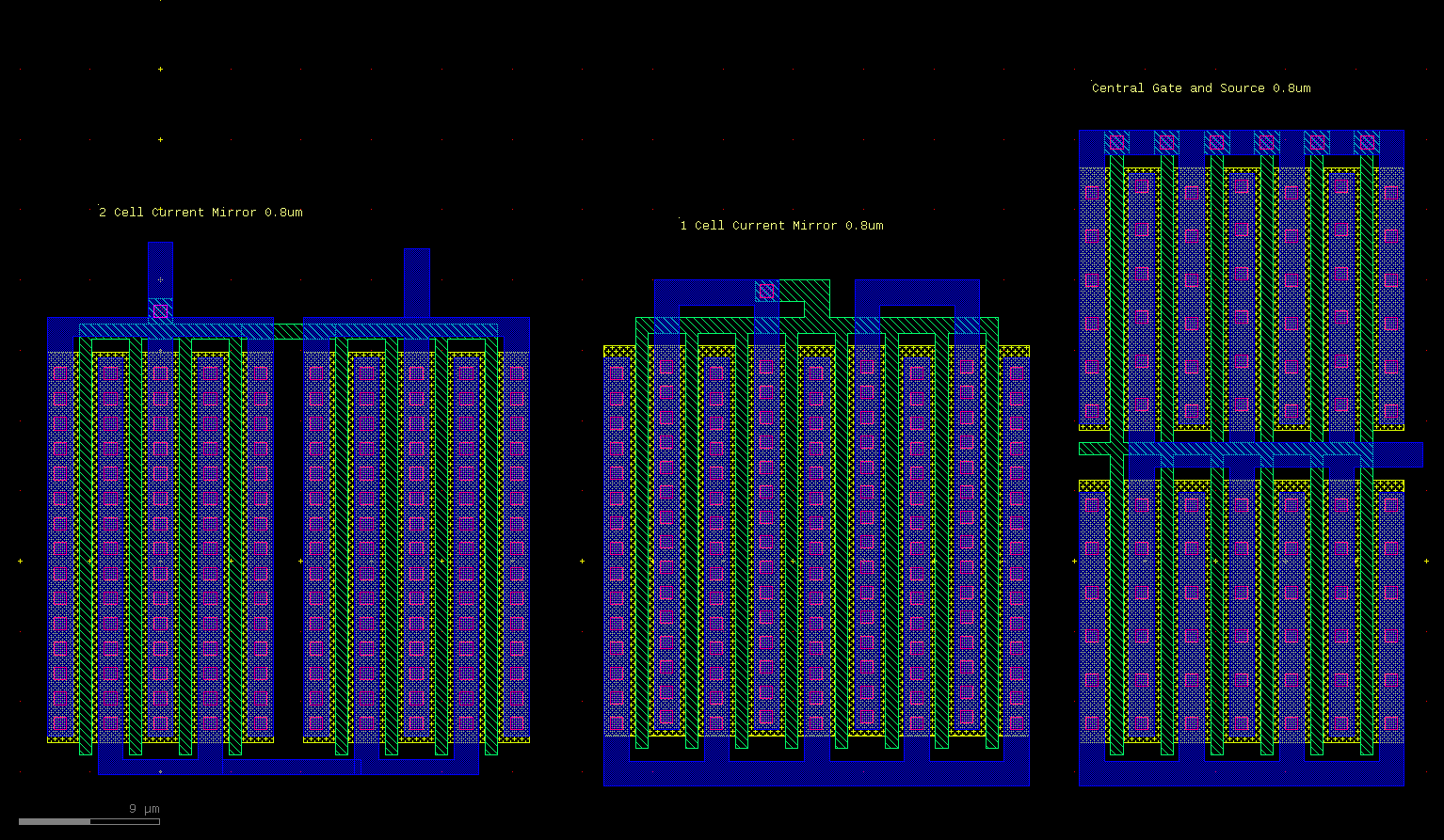
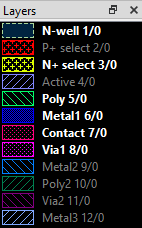
The first circuit I made a layout for was a simple NMOS current mirror. The schematic for the circuit can be seen in Figure 1. I made three different masks. The first of which made the current mirror using two separate devices. The second mask created the current mirror using an active region with separate sources. The third mask created the circuit using two active regions that utilize a common source, and a common gate. All of these layouts can be seen in Figure 2. The different layers of the masks are shown in Figure 3. The devices are all made using a 0.8um CMOS process. Reflecting on these layouts, I can see several areas for improvement. For instance, the first layout may not be very efficient in its use of space, and the third layout could benefit from better symmetry to enhance performance. Additionally, I did not include any well taps in any of the layouts, which could lead to issues with latch-up in a real-world application. There could also be improvements made to the gates of the transistors to reduce resistance and improve matching between the transistors. These layouts were all made without any design rule checking, which is something I plan to address in the next phase of this project.
These transistors are constructed using multiple fingers to reduce the overall width of each transistor. This approach reduces the total layout area while maintaining the overall gate area of the devices. Effectively, this is equivalent to having multiple transistors in parallel, which also helps to reduce the effects of variations in the manufacturing process on the performance of the transistors. The width of the transistors was designed to be 100µm with a gate length of 0.8µm. Given that both sides of the circuits have the same width, the output current will be a 1:1 copy of the reference current.
DRC Development
The problem
While working on a layout after completing question 7 at the end of chapter 3 in the textbook, I began designing the circuit layout. I then realized that creating the layout would be ineffective if I could not verify it against design rules. This led to another realization: I did not have a full set of design rules, and that the software I was using initially (LayoutEditor) did not have a DRC function. So I switched to KLayout, which does have DRC functionality, but I still needed to create the DRC files for the different CMOS processes I was working with.
Current Status
After some research, I was able to find a set of design rules for a 0.18µm process. Using the information from those design rules, I was able to create a rudimentary DRC file for the 0.18µm CMOS process. From there, I scaled the dimensions to create DRC files for the 0.8µm, 0.35µm, and 45nm CMOS processes.
DRC File Example
Below is an example of the 0.18µm CMOS DRC file I created. You can scroll through the file to see the various design rules and constraints. This file is still relatively basic, but since I don't have access to actual manufacturing design rules, it will suffice for practicing the layout of basic circuits.
# 0.18µm CMOS Design Rules Check (DRC) File
# ===============================
# 0.18 µm CMOS DRC (Ruby, KLayout)
# Scaffold v0.1 — structure first, rules later
# ===============================

report("0p18um")

# -------------------------------
# Layer input definitions
# -------------------------------
nwell    = input(  1, 0)    # N-Well
nimp     = input(  2, 0)    # N+ implant
pimp     = input(  3, 0)    # P+ implant
active   = input(  4, 0)    # Diffusion/Active
poly     = input(  5, 0)    # Polysilicon

# Metals
metal1   = input( 8, 0)
metal2   = input( 10, 0)
metal3   = input( 12, 0)
metal4   = input( 14, 0)
metal5   = input( 16, 0)
metal6   = input( 18, 0)

# Cuts and vias

cont_a   = input( 6, 0)    # Contact from M1 to Active
cont_p   = input( 7, 0)    # Contact from M1 to Poly
via1     = input( 9, 0)    # M1 <-> M2
via2     = input( 11, 0)    # M2 <-> M3
via3     = input( 13, 0)    # M3 <-> M4
via4     = input( 15, 0)    # M4 <-> M5
via5     = input( 17, 0)    # M5 <-> M

# -------------------------------
# Single-Layer Rules
# -------------------------------

# === N-Well ===
nwell_narrow = nwell.width("<", 1.0)
nwell_narrow.output("NW.W.1", "N-Well width < 1.0 µm")

nwell_close = nwell.space("<", 1.4)
nwell_close.output("NW.S.1", "N-Well spacing < 1.4 µm")

# === N+ Implant ===
nimp_narrow = nimp.width("<", 0.48)
nimp_narrow.output("NIMP.W.1", "N+ implant width < 0.48 µm")

nimp_close = nimp.space("<", 0.48)
nimp_close.output("NIMP.S.1", "N+ implant spacing < 0.48 µm")

nimp_small_area = nimp.with_area("<", 0.36)
nimp_small_area.output("NIMP.A.1", "N+ implant area < 0.36 µm²")

# === P+ Implant ===
pimp_narrow = pimp.width("<", 0.48)
pimp_narrow.output("PIMP.W.1", "P+ implant width < 0.48 µm")

pimp_close = pimp.space("<", 0.48)
pimp_close.output("PIMP.S.1", "P+ implant spacing < 0.48 µm")

pimp_small_area = pimp.with_area("<", 0.36)
pimp_small_area.output("PIMP.A.1", "P+ implant area < 0.36 µm²")

# === Active ===
diff_narrow = active.width("<", 0.28)
diff_narrow.output("active.W.1", "Active width < 0.28 µm")

diff_close = active.space("<", 0.32)
diff_close.output("active.S.1", "Active spacing < 0.32 µm")

# === Poly ===
poly_narrow = poly.width("<", 0.18)
poly_narrow.output("POLY.W.1", "Poly width < 0.18 µm")

poly_close = poly.space("<", 0.28)
poly_close.output("POLY.S.1", "Poly spacing < 0.28 µm")

# === Metal 1 – 4 ===
[metal1, metal2, metal3, metal4].each_with_index do |metal, i|
  layer = i + 1
  metal_narrow = metal.width("<", 0.32)
  metal_narrow.output("M#{layer}.W.1", "Metal#{layer} width < 0.32 µm")

  metal_close = metal.space("<", 0.32)
  metal_close.output("M#{layer}.S.1", "Metal#{layer} spacing < 0.32 µm")

  metal_small_area = metal.with_area("<", 0.2)
  metal_small_area.output("M#{layer}.A.1", "Metal#{layer} area < 0.2 µm²")
end

# === Metal 5 – 6 ===
[metal5, metal6].each_with_index do |metal, i|
  layer = i + 5
  metal_narrow = metal.width("<", 0.64)
  metal_narrow.output("M#{layer}.W.1", "Metal#{layer} width < 0.64 µm")

  metal_close = metal.space("<", 0.64)
  metal_close.output("M#{layer}.S.1", "Metal#{layer} spacing < 0.64 µm")
end

# ----------------------------------------
# CUT TO ACTIVE (cont_a)
# ----------------------------------------

# Minimum width/height
ct_a_small = cont_a.width("<", 0.24) | cont_a.height("<", 0.24)
ct_a_small.output("CT-A.DIM.1", "Cut-to-active width/height < 0.24 µm")

# Minimum spacing
ct_a_close = cont_a.space("<", 0.32)
ct_a_close.output("CT-A.S.1", "Cut-to-active spacing < 0.32 µm")

# Minimum overlap to Active
ct_a_act_encl = cont_a.enclosed_by(active, 0.04, projection: true)
(cont_a - ct_a_act_encl).output("CT-A.E.ACT.1",
  "Cut-to-active not enclosed by Active by ≥ 0.04 µm")

# Minimum overlap to Metal1
ct_a_m1_encl = cont_a.enclosed_by(metal1, 0.02, projection: true)
(cont_a - ct_a_m1_encl).output("CT-A.E.M1.1",
  "Cut-to-active not enclosed by Metal1 by ≥ 0.02 µm")

# ----------------------------------------
# CUT TO POLY (cont_p)
# ----------------------------------------

# Minimum width/height
ct_p_small = cont_p.width("<", 0.24) | cont_p.height("<", 0.24)
ct_p_small.output("CT-P.DIM.1", "Cut-to-poly width/height < 0.24 µm")

# Minimum spacing
ct_p_close = cont_p.space("<", 0.32)
ct_p_close.output("CT-P.S.1", "Cut-to-poly spacing < 0.32 µm")

# Minimum overlap to Poly
ct_p_poly_encl = cont_p.enclosed_by(poly, 0.04, projection: true)
(cont_p - ct_p_poly_encl).output("CT-P.E.POLY.1",
  "Cut-to-poly not enclosed by Poly by ≥ 0.04 µm")

# Minimum overlap to Metal1
ct_p_m1_encl = cont_p.enclosed_by(metal1, 0.02, projection: true)
(cont_p - ct_p_m1_encl).output("CT-P.E.M1.1",
  "Cut-to-poly not enclosed by Metal1 by ≥ 0.02 µm")

# Forbidden over Active
ct_p_over_active = cont_p & active
ct_p_over_active.output("CT-P.FORB.ACT.1",
  "Cut-to-poly is not allowed over Active")

# ----------------------------------------
# VIA1, VIA2, VIA3 (same rules)
# ----------------------------------------

[
  [via1, metal1, metal2, 1],
  [via2, metal2, metal3, 2],
  [via3, metal3, metal4, 3]
].each do |via, lower, upper, idx|

  # Minimum width/height
  via_small = via.width("<", 0.32) | via.height("<", 0.32)
  via_small.output("V#{idx}.DIM.1", "Via#{idx} width/height < 0.32 µm")

  # Minimum spacing
  via_close = via.space("<", 0.32)
  via_close.output("V#{idx}.S.1", "Via#{idx} spacing < 0.32 µm")

  # Lower metal enclosure
  via_lower_encl = via.enclosed_by(lower, 0.08, projection: true)
  (via - via_lower_encl).output("V#{idx}.E.LOW.1",
    "Via#{idx} not enclosed by lower metal by ≥ 0.08 µm")

  # Upper metal enclosure
  via_upper_encl = via.enclosed_by(upper, 0.04, projection: true)
  (via - via_upper_encl).output("V#{idx}.E.UP.1",
    "Via#{idx} not enclosed by upper metal by ≥ 0.04 µm")
end

# ----------------------------------------
# VIA4 (metal4 ↔ metal5)
# ----------------------------------------

# Minimum width/height
via4_small = via4.width("<", 0.32) | via4.height("<", 0.32)
via4_small.output("V4.DIM.1", "Via4 width/height < 0.32 µm")

# Minimum spacing
via4_close = via4.space("<", 0.32)
via4_close.output("V4.S.1", "Via4 spacing < 0.32 µm")

# Lower metal enclosure (metal4)
via4_lower_encl = via4.enclosed_by(metal4, 0.16, projection: true)
(via4 - via4_lower_encl).output("V4.E.LOW.1",
  "Via4 not enclosed by Metal4 by ≥ 0.16 µm")

# Upper metal enclosure (metal5)
via4_upper_encl = via4.enclosed_by(metal5, 0.08, projection: true)
(via4 - via4_upper_encl).output("V4.E.UP.1",
  "Via4 not enclosed by Metal5 by ≥ 0.08 µm")

# ----------------------------------------
# VIA5 (metal5 ↔ metal6)
# ----------------------------------------

# Minimum width/height
via5_small = via5.width("<", 0.6) | via5.height("<", 0.6)
via5_small.output("V5.DIM.1", "Via5 width/height < 0.6 µm")

# Minimum spacing
via5_close = via5.space("<", 0.6)
via5_close.output("V5.S.1", "Via5 spacing < 0.6 µm")

# Lower metal enclosure (metal5)
via5_lower_encl = via5.enclosed_by(metal5, 0.02, projection: true)
(via5 - via5_lower_encl).output("V5.E.LOW.1",
  "Via5 not enclosed by Metal5 by ≥ 0.02 µm")

# Upper metal enclosure (metal6)
via5_upper_encl = via5.enclosed_by(metal6, 0.02, projection: true)
(via5 - via5_upper_encl).output("V5.E.UP.1",
  "Via5 not enclosed by Metal6 by ≥ 0.02 µm")

# ----------------------------------------
# ACTIVE REGION RULES
# ----------------------------------------

gate = active & poly

# Minimum gate length: 0.18 µm
gate_short = gate.width("<", 0.18)
gate_short.output("GATE.L.1", "Gate length < 0.18 µm")

# Poly overshoot over active: 0.2 µm
poly_overshoot = gate.enclosed_by(poly, 0.2, projection: true)
(gate - poly_overshoot).output("GATE.O.1",
  "Poly overshoot over active < 0.2 µm")

gate_width = gate.height("<", 0.28)
gate_width.output("GATE.W.1", "Gate width < 0.28 µm")

# Poly spacing to implant edge: 0.4 µm
poly_to_implant = poly.space(nimp | pimp, "<", 0.4)
poly_to_implant.output("POLY.IMP.S.1",
  "Poly spacing to implant < 0.4 µm")

gate_to_active_edge = gate.space(active, "<", 0.36)
gate_to_active_edge.output("GATE.ACT.S.1",
  "Gate spacing to active edge < 0.36 µm")

poly_outside_active = poly - gate
poly_outside_to_active = poly_outside_active.space(active, "<", 0.16)
poly_outside_to_active.output("POLY.ACT.S.1",
  "Poly outside active spacing to active < 0.16 µm")

poly_to_cont_a = poly.space(cont_a, "<", 0.14)
poly_to_cont_a.output("POLY.CT-A.S.1",
  "Poly spacing to cut-to-active < 0.14 µm")

active_to_cont_p = active.space(cont_p, "<", 0.14)
active_to_cont_p.output("ACT.CT-P.S.1",
  "Active spacing to cut-to-poly < 0.14 µm")

nwell_to_active = nwell.space(active, "<", 0.4)
nwell_to_active.output("NW.ACT.S.1",
  "Nwell spacing to active < 0.4 µm")

cont_a_to_implant = cont_a.space(nimp | pimp, "<", 0.2)
cont_a_to_implant.output("CT-A.IMP.S.1",
  "Cut-to-active spacing to implant < 0.2 µm")

# Implant overlap over active: 0.26 µm
nimp_encl = active.enclosed_by(nimp, 0.26, projection: true)
(active - nimp_encl).output("NIMP.ACT.E.1",
  "N+ implant overlap over active < 0.26 µm")

pimp_encl = active.enclosed_by(pimp, 0.26, projection: true)
(active - pimp_encl).output("PIMP.ACT.E.1",
  "P+ implant overlap over active < 0.26 µm")
2025/12/23
DRC Update
After beginning to work on a layout, I finally had the chance to use the DRC tool, which gave me the chance to find the errors in the DRC code and debug them. Most of the errors were syntax errors and methods that do not exist in KLayout's DRC language. After fixing those errors, I was able to run the DRC tool successfully on my layouts, which I then used to find and fix the errors in the current layout. One error in the DRC file that I could not fix was regarding a rule that was intended to check for the minimum spacing between the active region and strips of poly that run parallel to the active region. This rule, however, kept flagging errors at the ends of the poly strips that made up the gate and were perpendicular to the edge of the active region. As a result, I had to remove that rule from the DRC file. Here is the updated DRC file that I have been using since fixing the initial errors.
# Updated 0.18µm CMOS Design Rules Check (DRC) File
# ===============================
# 0.18 µm CMOS DRC (Ruby, KLayout)
# Scaffold v0.1 — structure first, rules later
# ===============================

report("0p18um")

# -------------------------------
# Layer input definitions
# -------------------------------
nwell  = input(1, 0)
nimp   = input(2, 0)
pimp   = input(3, 0)
active = input(4, 0)
poly   = input(5, 0)

# Metals
metal1 = input(8, 0)
metal2 = input(10, 0)
metal3 = input(12, 0)
metal4 = input(14, 0)
metal5 = input(16, 0)
metal6 = input(18, 0)

# Cuts and vias
cont_a = input(6, 0)
cont_p = input(7, 0)
via1   = input(9, 0)
via2   = input(11, 0)
via3   = input(13, 0)
via4   = input(15, 0)
via5   = input(17, 0)

# -------------------------------
# Single-Layer Rules
# -------------------------------

# === N-Well ===
nwell.width(1.0).output("NW.W.1", "N-Well width < 1.0 µm")
nwell.space(1.4).output("NW.S.1", "N-Well spacing < 1.4 µm")

# === N+ Implant ===
nimp.width(0.48).output("NIMP.W.1", "N+ implant width < 0.48 µm")
nimp.space(0.48).output("NIMP.S.1", "N+ implant spacing < 0.48 µm")
nimp.with_area(0.36).output("NIMP.A.1", "N+ implant area < 0.36 µm²")

# === P+ Implant ===
pimp.width(0.48).output("PIMP.W.1", "P+ implant width < 0.48 µm")
pimp.space(0.48).output("PIMP.S.1", "P+ implant spacing < 0.48 µm")
pimp.with_area(0.36).output("PIMP.A.1", "P+ implant area < 0.36 µm²")

# === Active ===
active.width(0.28).output("active.W.1", "Active width < 0.28 µm")
active.space(0.32).output("active.S.1", "Active spacing < 0.32 µm")

# === Poly ===
poly.width(0.18).output("POLY.W.1", "Poly width < 0.18 µm")
poly.space(0.28).output("POLY.S.1", "Poly spacing < 0.28 µm")

# === Metal 1–4 ===
[metal1, metal2, metal3, metal4].each_with_index do |m, i|
  idx = i + 1
  m.width(0.32).output("M#{idx}.W.1", "Metal#{idx} width < 0.32 µm")
  m.space(0.32).output("M#{idx}.S.1", "Metal#{idx} spacing < 0.32 µm")
  m.with_area(0.2).output("M#{idx}.A.1", "Metal#{idx} area < 0.2 µm²")
end

# === Metal 5–6 ===
[metal5, metal6].each_with_index do |m, i|
  idx = i + 5
  m.width(0.64).output("M#{idx}.W.1", "Metal#{idx} width < 0.64 µm")
  m.space(0.64).output("M#{idx}.S.1", "Metal#{idx} spacing < 0.64 µm")
end

# ----------------------------------------
# CUT TO ACTIVE (cont_a)
# ----------------------------------------

cont_a.width(0.24).output("CT-A.DIM.1", "Cut-to-active width/height < 0.24 µm")
cont_a.space(0.32).output("CT-A.S.1", "Cut-to-active spacing < 0.32 µm")

cont_a.enclosed(active, 0.04)
  .output("CT-A.E.ACT.1", "Cut-to-active not enclosed by Active by ≥ 0.04 µm")

cont_a.enclosed(metal1, 0.02)
  .output("CT-A.E.M1.1", "Cut-to-active not enclosed by Metal1 by ≥ 0.02 µm")

# ----------------------------------------
# CUT TO POLY (cont_p)
# ----------------------------------------

cont_p.width(0.24).output("CT-P.DIM.1", "Cut-to-poly width/height < 0.24 µm")
cont_p.space(0.32).output("CT-P.S.1", "Cut-to-poly spacing < 0.32 µm")

cont_p.enclosed(poly, 0.04)
  .output("CT-P.E.POLY.1", "Cut-to-poly not enclosed by Poly by ≥ 0.04 µm")

cont_p.enclosed(metal1, 0.02)
  .output("CT-P.E.M1.1", "Cut-to-poly not enclosed by Metal1 by ≥ 0.02 µm")

(cont_p & active)
  .output("CT-P.FORB.ACT.1", "Cut-to-poly is not allowed over Active")

# ----------------------------------------
# VIA1, VIA2, VIA3
# ----------------------------------------

[
  [via1, metal1, metal2, 1],
  [via2, metal2, metal3, 2],
  [via3, metal3, metal4, 3]
].each do |via, lower, upper, idx|

  via.width(0.32).output("V#{idx}.DIM.1", "Via#{idx} width/height < 0.32 µm")
  via.space(0.32).output("V#{idx}.S.1", "Via#{idx} spacing < 0.32 µm")

  via.enclosed(lower, 0.08)
    .output("V#{idx}.E.LOW.1", "Via#{idx} not enclosed by lower metal by ≥ 0.08 µm")

  via.enclosed(upper, 0.04)
    .output("V#{idx}.E.UP.1", "Via#{idx} not enclosed by upper metal by ≥ 0.04 µm")
end

# ----------------------------------------
# VIA4
# ----------------------------------------

via4.width(0.32).output("V4.DIM.1", "Via4 width/height < 0.32 µm")
via4.space(0.32).output("V4.S.1", "Via4 spacing < 0.32 µm")

via4.enclosed(metal4, 0.16)
  .output("V4.E.LOW.1", "Via4 not enclosed by Metal4 by ≥ 0.16 µm")

via4.enclosed(metal5, 0.08)
  .output("V4.E.UP.1", "Via4 not enclosed by Metal5 by ≥ 0.08 µm")

# ----------------------------------------
# VIA5
# ----------------------------------------

via5.width(0.6).output("V5.DIM.1", "Via5 width/height < 0.6 µm")
via5.space(0.6).output("V5.S.1", "Via5 spacing < 0.6 µm")

via5.enclosed(metal5, 0.02)
  .output("V5.E.LOW.1", "Via5 not enclosed by Metal5 by ≥ 0.02 µm")

via5.enclosed(metal6, 0.02)
  .output("V5.E.UP.1", "Via5 not enclosed by Metal6 by ≥ 0.02 µm")

# ----------------------------------------
# ACTIVE REGION RULES
# ----------------------------------------

gate = active & poly

gate.width(0.18).output("GATE.L.1", "Gate length < 0.18 µm")

active.enclosed(poly, 0.2)
  .output("GATE.O.1", "Poly overshoot over active < 0.2 µm")

gate.with_area(0.0504).width(0.28)
    .output("GATE.W.1", "Gate width < 0.28 µm")

poly.separation(nimp, 0.4)
    .output("POLY.IMP.S.1A", "Poly spacing to N+ implant < 0.4 µm")

poly.separation(pimp, 0.4)
    .output("POLY.IMP.S.1B", "Poly spacing to P+ implant < 0.4 µm")

gate.separation(active, 0.36)
  .output("GATE.ACT.S.1", "Gate spacing to active edge < 0.36 µm")

poly.separation(cont_a, 0.14)
  .output("POLY.CT-A.S.1", "Poly spacing to cut-to-active < 0.14 µm")

active.separation(cont_p, 0.14)
  .output("ACT.CT-P.S.1", "Active spacing to cut-to-poly < 0.14 µm")

nwell.separation(active, 0.4)
  .output("NW.ACT.S.1", "Nwell spacing to active < 0.4 µm")

cont_a.separation(nimp | pimp, 0.2)
  .output("CT-A.IMP.S.1", "Cut-to-active spacing to implant < 0.2 µm")

active.enclosed(nimp, 0.26)
  .output("NIMP.ACT.E.1", "N+ implant overlap over active < 0.26 µm")

active.enclosed(pimp, 0.26)
  .output("PIMP.ACT.E.1", "P+ implant overlap over active < 0.26 µm")
2025/12/29
LVS Development
The next step in this project is to begin developing layout versus schematic (LVS) scripts to fully verify my layouts. This will involve creating netlists from both the schematic and layout, and then comparing them to ensure they match. This is a crucial step in the verification process, as it ensures that the layout accurately represents the intended circuit design. You can see the script I have made down below. As I am new to writing LVS scripts and I am just beginning this project, I expect that this script is just going to be a starting point. As I change the script and improve it, I will add it in future updates on this page.
              # ======================================== # LVS – analog CMOS
              (KLayout + LTspice) # ========================================
              report("lvs_report") # --- 1. Layer mapping (replace with your
              real GDS numbers) --- nwell = input( 1, 0) # N-Well nimp = input(
              2, 0) # N+ implant pimp = input( 3, 0) # P+ implant active =
              input( 4, 0) # Diffusion/Active poly = input( 5, 0) # Polysilicon
              cont_a = input( 6, 0) # Contact from M1 to Active cont_p = input(
              7, 0) # Contact from M1 to Poly metal1 = input( 8, 0) via1 =
              input( 9, 0) # M1 <-> M2 metal2 = input(10, 0) via2 = input(11, 0)
              # M2 <-> M3 metal3 = input(12, 0) via3 = input(13, 0) # M3 <-> M4
              metal4 = input(14, 0) via4 = input(15, 0) # M4 <-> M5 metal5 =
              input(16, 0) via5 = input(17, 0) # M5 <-> M6 metal6 = input(18, 0)
              # --- 2. Connectivity --- # Contacts to M1 connect(cont_a, active,
              metal1) connect(cont_p, poly, metal1) # Vias between metals
              connect(via1, metal1, metal2) connect(via2, metal2, metal3)
              connect(via3, metal3, metal4) connect(via4, metal4, metal5)
              connect(via5, metal5, metal6) # You can also define
              "connect(metal1, metal1)" if slotting or OPC breaks shapes # ---
              3. Device recognition --- gate = active & poly # NMOS in P-well
              (no nwell) with N+ implant nmos_active = active & nimp & ~nwell
              nmos_gate = gate & nmos_active nmos_sd = nmos_active - nmos_gate #
              PMOS in N-well with P+ implant pmos_active = active & pimp & nwell
              pmos_gate = gate & pmos_active pmos_sd = pmos_active - pmos_gate #
              NMOS devices nmos_devs = nmos_gate.device( nmos_sd, # source/drain
              poly, # gate conductor nil, # bulk (we'll infer from well) "nmos"
              # device name to match SPICE ) # PMOS devices pmos_devs =
              pmos_gate.device( pmos_sd, poly, nwell, # bulk in N-well "pmos" )
              # Simple poly resistor (between its two terminals) r_devs =
              rpoly.device( metal1, # first terminal where it connects to M1
              metal1, # second terminal (other end) nil, "R" # SPICE resistor
              name ) # Simple MIM capacitor between mim (top) and mim_bot
              (bottom) c_devs = mim.device( mim_bot, nil, nil, "C" # SPICE
              capacitor name ) # --- 4. Netlist extraction from layout ---
              layout_nl = extract_netlist("layout") # Optional: name mapping for
              global nets # map_nets(layout_nl, { "VDD" => "VDD!", "VSS" => "0"
              }) # --- 5. Read LTspice netlist --- # This file should contain
              .subckt matching the layout top cell name # e.g., .subckt
              opamp_core INP INN OUT VDD VSS schematic_nl =
              read_netlist("opamp_core.spice", "schematic") # --- 6. Device and
              net mapping if names differ --- # Example if LTspice uses
              different names: # map_devices(schematic_nl, layout_nl, { "M" =>
              "nmos", "Mp" => "pmos" }) # map_nets(schematic_nl, layout_nl, {
              "0" => "VSS" }) # --- 7. Perform LVS comparison ---
              compare(schematic_nl, layout_nl)
2025/12/24
Completed Circuits
Please check out the circuits I have completed so far:
More circuits will be added as they are completed.
Next Steps
Now that the DRC and LVS files are complete, I can resume working on solving the end-of-chapter questions from the textbook and creating layouts for them. With the DRC and LVS checks in place, I can resonably ensure that my layouts are releasitaclly correct and adhere to design rules. This will greatly enhance the learning experience and help me develop real-world skills in circuit design and layout.