Circuit Overview
This page provides a detailed analysis and layout implementation of a circuit from Chapter 3, Problem 10 of "Analog Integrated Circuit Design" by Carusone, Johns, and Martin. This exercise is part of my ongoing project to deepen my understanding of analog circuit design principles and practice with industry-standard design tools.
Problem Statement
Chapter 3, Problem 10: Design a common-source amplifier with active load using the 0.18µm device parameters provided in the textbook. Assume a supply voltage of 1.8V, and that the amplifier only consumes 1mW of power. The gain of the amplifier should be at least 5[V/V]. Make sure that each transistor has Veff = 0.25V and that the gate length is L = 0.26µm.
Design Parameters
The requirements of the design are summarized as follows:
- Amplifier style - Common-Source
- Supply Voltage (VDD) = 1.8V
- Power Consumption = 1mW
- Minimum Gain (Av) = -5 V/V
- Transistor Effective Voltage (Veff) = 0.25V
- Transistor Gate Length (L) = 0.26µm
0.18µm Technology Parameters
These are the values provided by the textbook for the 0.18µm process technology.
- µnCox = 270 µA/V²
- µpCox = 70 µA/V²
- Vtn = 0.45V
- Vtp = -0.45V
- λ*L = 0.08 µm/V
Circuit Analysis
Analysis Approach
The first step in designing this amplifier is to determine what the current through the circuit needs to be. Given the power consumption requirement of 1mW and the supply voltage of 1.8V we can calculate the current as follows:
P = V × I ⟹ I = P / V
Where I is the total current drawn from the supply. Since there will be 2 branches in the circuit that will draw the same magnitude of current we can use the formula:
I = P / 2V
Plugging in the values we get: I = 278µA.
NMOS Transistor Design
Next, we can use the current to determine the small signal resistance of the transistors on the amplifying side of the circuit. The small signal resistance, rds, is given by:
rds = 1 / λID = L / (λ*L * ID)
Plugging in the values we get: rdsn = rdsp = 11.69kΩ. From here we can use the formula for gain in a common-source amplifier with an active load to use the transconductance, gm, to determine the minimum gate width of the NMOS transistor. The gain is given by:
Av = -gm × (rdsn || rdsp) = -gm × (rdsn/2)
Rearranging for gm we get: gmmin = 854.7µA/V. Utilizing the formula for transconductance in the saturation region, we can solve for the minimum gate width, Wmin: 1.26µm. However, to ensure that the design meets the required Veff of 0.25V, we will solve the equation for Ids to find the required gate width. As long as this calculated width is larger than Wmin, we will be able to meet both requirements. With Ids set to 278µA and Veff set to 0.25V, we find that W = 8.56µm, which results in a voltage gain of approximately -13 V/V, which satisfies our gain requirement. Finally, for the design of the NMOS to be complete, I should mention that the input voltage applied to the NMOS gate must have a DC offset of at least Vtn + Veff = 0.7V to ensure that the transistor is operating in saturation, and that the input signal is being amplified.
PMOS Transistor Design
The design of the PMOS transistors is fairly straightforward since the current through both PMOS is the same, and the effective voltage requirement is predetermined, we can directly solve for the gate width. Using the same formula for Ids as before, we find that W = 33.04µm. Finally, to make sure that the transistors in the current mirror are operating in saturation, I added a resistor in series with the biasing PMOS transistor. The resistor value is determined by using the effective voltage, the power supply voltage, and the threshold voltage to find the voltage drop across the PMOS transistor while it is in saturation. From there, the resistor value is found by dividing the PMOS drain voltage by the current through the branch. Which results in a calculated resistor value of 3.96kΩ. After performing a simulation of the circuit in LTSpice I found that a resistor value of 3.98kΩ resulted in the desired operating point.
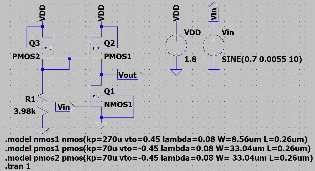
Final Circuit Design
The final circuit design is shown in figure 1 below.
KLayout Implementation
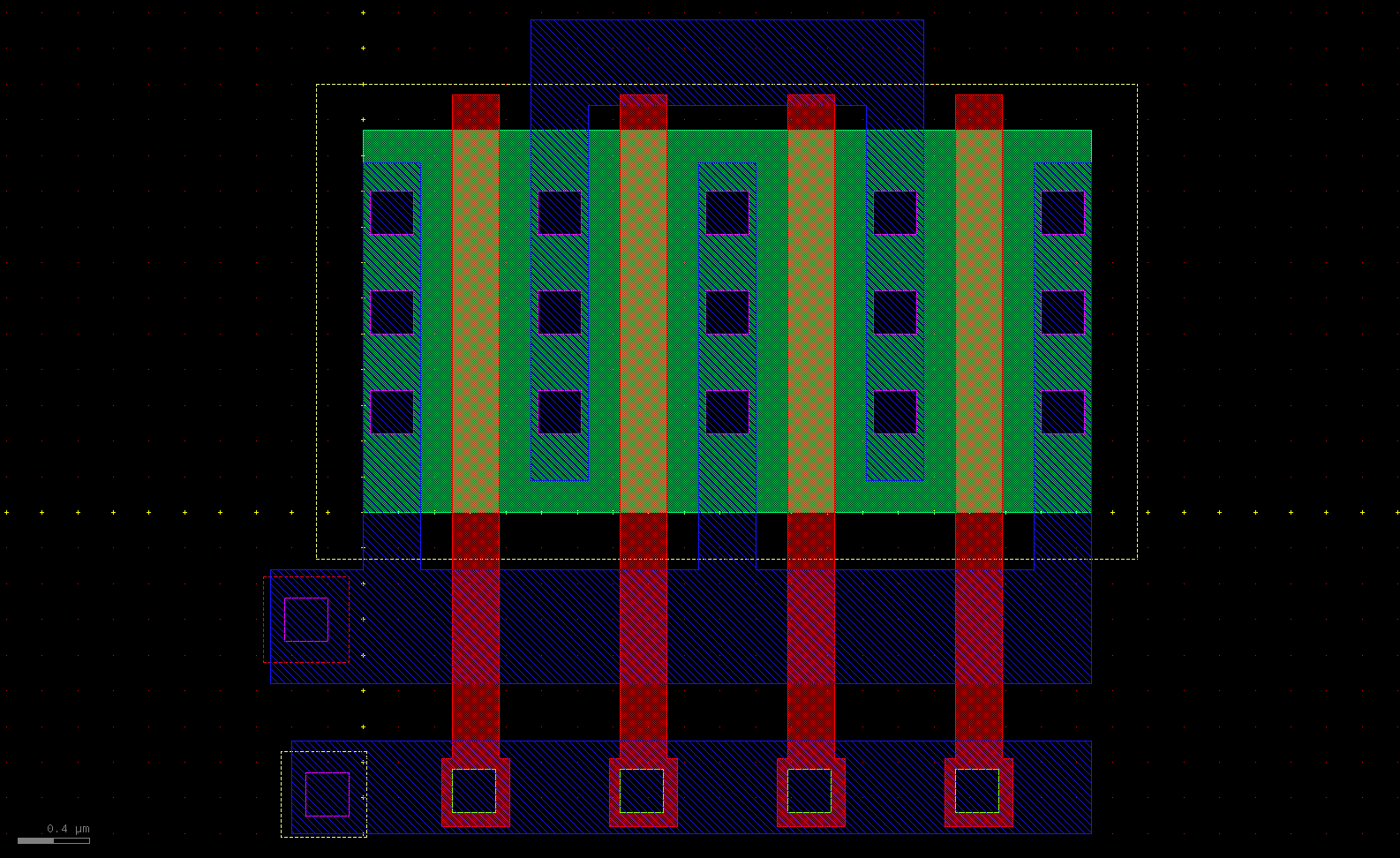
For this layout implementation, I decided to not just make a layout of the circuit schematic. Instead, I decided to go beyond that and create a layout that includes 4 instances of the common-source amplifier that could theoretically be turned into a proper tapeout for fabrication. This required additional considerations such as adding proper electrostatic discharge (ESD) circuit protection, and connection pads for inputs, outputs, and power supply. The full layout is shown in figure 2 below.
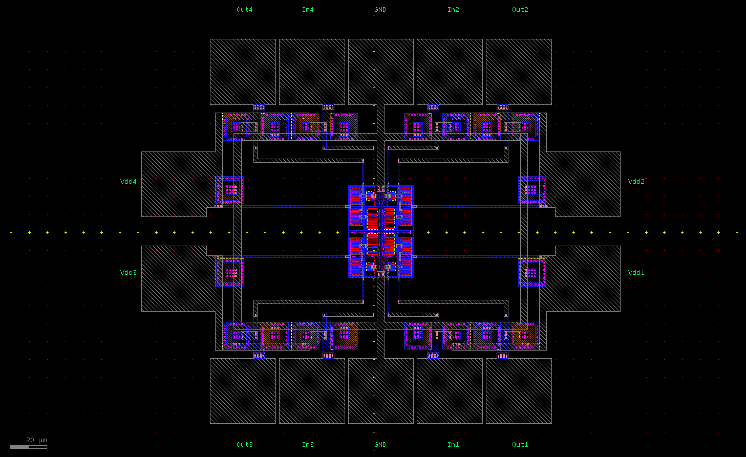
Figure 2 shows the full layout of the design, which includes 4 instances of the common-source amplifier. Each amplifier instance is connected to its own input, output, and voltage supply pads. To save some space, I kept the ground pads shared between all 4 amplifiers. I made two grounding pads so that there was a ground connection on either side of the chip. The ground pads are connected so that either pad can be used as a ground reference. This final setup fits in a 10 pin package.
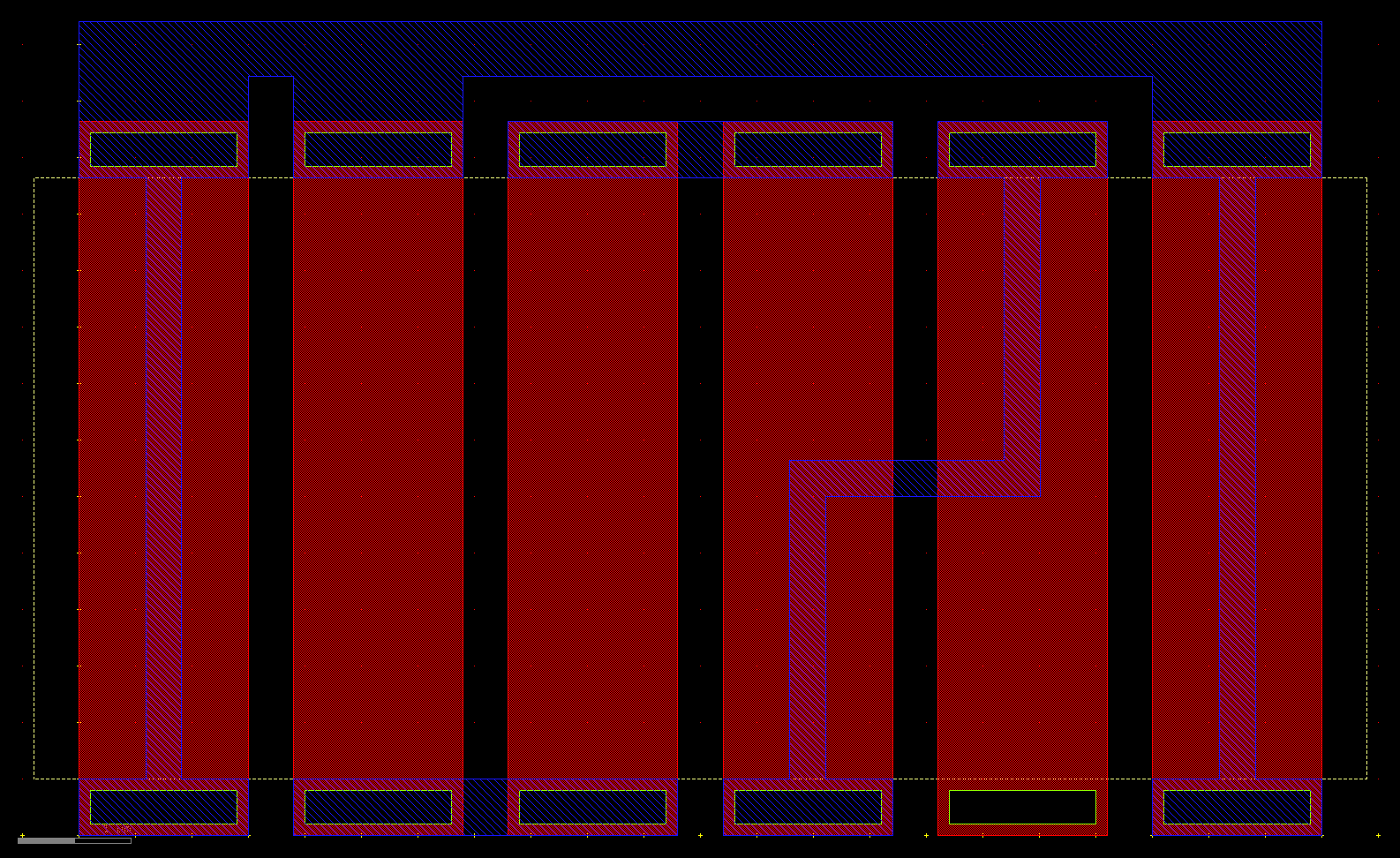
Amplifier Layout
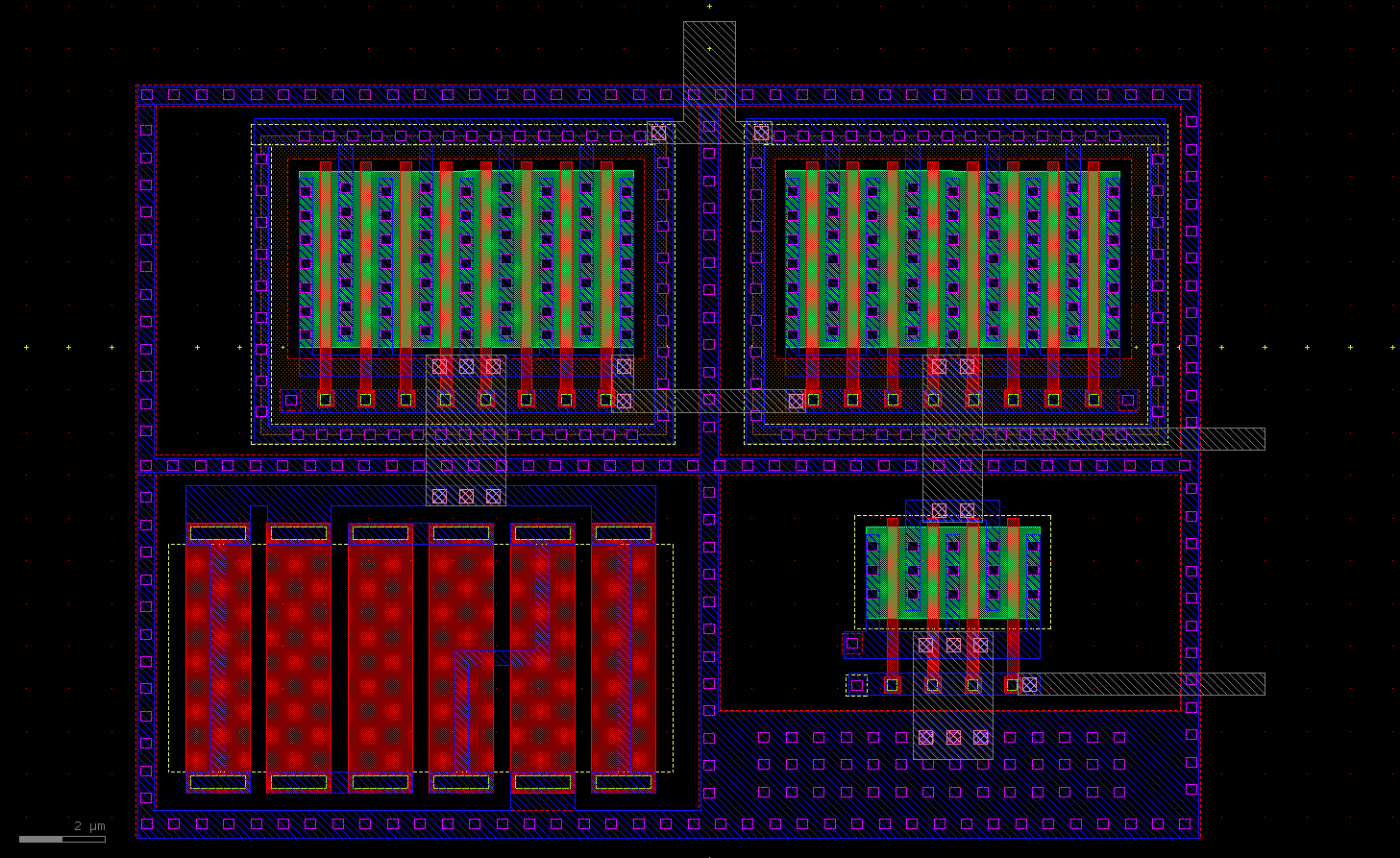
Now let's look at the layout of the individual common-source amplifier instances, shown above in figure 3. From the figure you can see that the layout has three distinct sections. The current mirror and active load PMOS transistors can be seen at the top of the layout. The NMOS section is in the bottom right corner, and the passive resistive load is in the bottom left corner. All around the layout there is a series of substrate contacts that are connected to ground. This achieves a couple of things: first, it connects the body of the NMOS transistor to ground. But more importantly, it helps to isolate the circuit from any unwanted noise and interference that is transmitted through the substrate. Which means that each circuit should be able to operate without interfering with each other.
PMOS Design
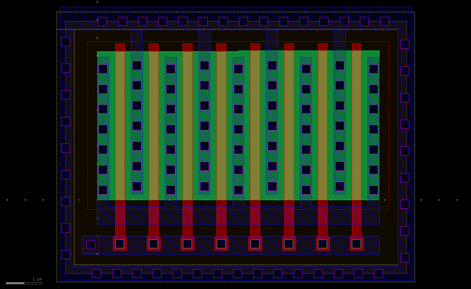
Focusing in on the PMOS section of the layout, the PMOS transistors are identical, and so only one needed to be designed. I then just mirrored the instance about the vertical axis to create the second PMOS transistor. One particular design choice I made here was to use two slightly different gate widths for the PMOS transistor. As the calculated gate width was 33.04µm, and my design choice of using 8 fingers resulted in a gate width 4.13µm per finger. Since the grid size I am using is 0.02µm, I decided it was better to stick to the grid. So I made 4 of the fingers 4.12µm wide, and the other 4 fingers 4.14µm wide. This maintained the overall gate area while reducing the overall layout size. To reduce the chances of damaging the gate oxide during fabrication, I separated each of the gates and connected them using a strip of metal 1, which was then connected to the substrate using a NAC diode. One more important design choice I made here was to extend the source of the PMOS so that it surrounded the entirety of the Nwell, with well contacts placed at regular intervals. This does two things: first, it connects the body of the PMOS to the highest potential in the circuit. The second thing is that the ring of well contacts around the transistor helps to isolate the transistor from unwanted substrate noise and interference.
NMOS Design
Moving on to the NMOS section of the layout shown in figure 5 above, it was the last active component to be designed. It also is the component that I am least satisfied with. The final dimensions of the NMOS transistor are way smaller than any of the other components, which results in a lot of wasted space. While I don't believe it is necessarily wrongly designed, I do think that there is a better way to utilize the space. The problem is that most of the space is wasted in the horizontal direction. I could utilize this by rotating the transistor 90 degrees and simply making a single-finger transistor. This would allow for a more compact layout. However, it risks having matching issues between the NMOS and PMOS transistors, since their poly layers would be oriented differently, which would result in different etching results in fabrication. So I decided to stick with the multi-finger approach and to use as many fingers as reasonably possible to make sure the transistor makes as much use of the available space. Another problem I have with this NMOS design is I'm not sure if I should have extended the source region to surround the transistor and to add well contacts. This would have added some redundancy to the isolation of the transistor from substrate noise. But as there was already a grounding region around the entire amplifier layout, I decided it wasn't necessary.
Resistive Load Design
The last part of the amplifier layout was the resistive load on the biasing side of the circuit. For this, I used a strip of poly with an N+ implantation region as the body of the resistor. I assumed a sheet resistance of 250Ω/sq for this type of resistor. It was easiest to break up the 3.98kΩ resistor into 4 resistors of 995Ω each. This reduced the amount of vertical space that the resistors took up. However, I did add some dummy resistors on the sides of the resistor to help with matching the actual resistors. But this resulted in a resistor setup that was wider than the PMOS component. So there is some wasted space here as well. I chose to use a passive resistive load instead of an active load to reduce the amount of noise in the circuit, as well as to have an accurate and stable resistance value. So, in order to achieve 4 resistors with the value of 995Ω, I designed each resistor to have a body length of 5.32µm with a standardized width of 1.5µm
Design Notes
One design rule that I haven't really mentioned yet is that I have decided to follow minimum resistor sizes. Given my main source of layout information is a 20-year-old book, I scaled the minimum resistor width from 5µm to 1.5µm, and the minimum resistor length from 10µm to 5µm. I might revisit this decision later, as even with this scaling, the resistors still increased the size of the layout significantly.
Design Rule Verification
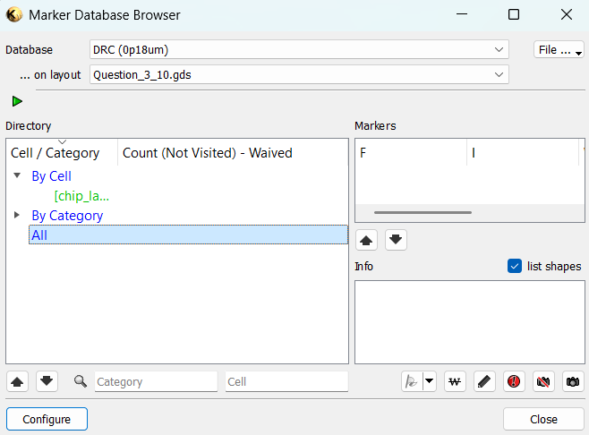
This layout was designed in accordance with the design rules I found for the 0.18µm technology process. To see the complete rules, please refer to the Project 1 page. The full DRC script I used can be found there. Using the built-in DRC verification tool in KLayout, I ran the DRC check on the layout. The results showed that there were no design rule violations.
01/13/2026