Projects
Post Assembly Thermal Annealing of Microelectromechanical Devices
The challenge present for this project was to design either a Microelectromechanical (MEMs) device, or a process for MEMs devices. My team and I responded to the challenge by designing a process for the thermal annealing of MEMs devices after they have been assembled. This allows for MEMs designers to create 2D designs that can then be assembled into 3D structures. Then once the structures are assembled, they can be hardened in place to provide extra stability and strength.
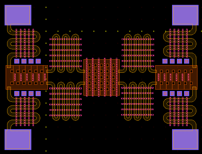
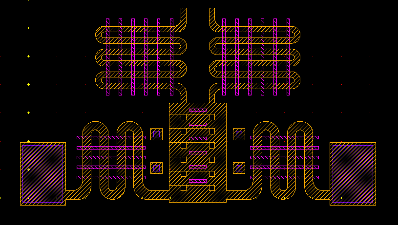
To achieve this, we created a bridge using 2 Tsang suspensions that act as the base of the bridge and support the main platform. The main platform is suspended from the Tsang suspensions using springs that act in a similar manner to the springs at the base of the Tsang suspensions. From there we sputtered a layer of gold on top of the bridge after fabrication. This thin gold layer provides a conductive path that we then ran a current through, treating the springs supporting the structure as a resistor and thermal element. On the microscopic scale, the gold layer heats up in seconds. This heat is then transferred into the SU8 Photoresist, causing it to harden.
We were given 2 rounds of fabrication to test our design. In the first round of tests, we tried to test how the thickness of the springs would affect the time required to anneal the SU8 structure. But when we strayed away from having a thickness to width ratio of the springs of 1:3, we encountered issues with the springs either being too fragile or being so stiff the structure would not assemble. The thickness of the springs was the most important factor in the mechanical aspect of our design, as it limited our ability to assemble the structure and limited our ability to control the resistance of the springs to just the length of the springs.
Regardless of these challenges we were successful in our attempt to design a process that could be used to anneal MEMs devices after they have been assembled. Our design process also allows for specific parts of the structure to be hardened. By choosing where the voltage is applied to the structure, we can control where the current is passed through the gold layer. This allows for the selective hardening of parts of the structure, which can be used to create structures that require a stiff base and a flexible middle structure. Or to create an entire structure that needs to be hardened.
Project Reflection
Overall, this project provided valuable hands-on experience in the design and fabrication of MEMS devices, and I thoroughly enjoyed working through the complex challenges of micro-scale engineering. It reinforced the importance of considering both mechanical and electrical aspects in the design process, as well as the need for iterative testing and refinement. Beyond the engineering design aspects, I found learning about the photolithographic design and manufacturing processes particularly fascinating, as it provided deep insight into how modern microelectronic and MEMS devices are fabricated at the micro and nanoscale levels. The challenges faced during fabrication highlighted the complexities involved in working with micro-scale structures, and the need for precise control over material properties and dimensions. The experience of seeing our designs come to life through the fabrication process was both educational and rewarding, bridging the gap between theoretical knowledge and practical implementation in microfabrication technology.
PPG Sensor
Project Overview
The purpose of this project was to implement and apply the principles of the UBC course ENGR 451 Microelectronics 2. This project involved the amplification filtering, conditioning, and digitization of a PPG (Photoplethysmogram) signal. The PPG signal is a non-invasive method of measuring blood volume changes in the microvascular bed of tissue, and is commonly used in medical applications to monitor heart rate and blood oxygen levels. This project was also the focus of the course labs. With each lab focusing on a different aspect of the PPG sensor design. The first lab focused on lab safety and the use of the lab equipment such as the oscilloscope and power supply. So I won't go into detail about that lab.
Lab 2: Amplification
This is the part of the project where the design work really started.
To start this portion of the project, we began by creating an infrared
optical sensor assembly. A 940 nm infrared LED was used as the light
source, and a photodiode was used to detect the light. The LED and
photodiode were soldered onto a breadboard to create the assembly,
with wires connecting the components to the power supply and the rest
of the circuit. The LED was driven by a 5V power supply with an 82 Ohm
resistor in series to limit the current. The photodiode was connected
to an operational amplifier (op-amp) in a transimpedance configuration
to convert the current generated by the photodiode into a voltage
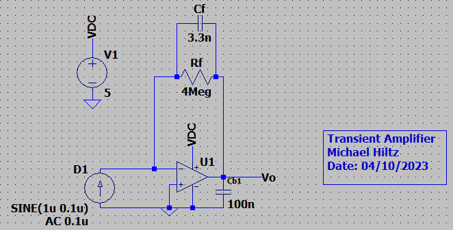
signal. The op-amp model used in this project was the MCP601, shown in
Figure 1 as U1. The photodiode is shown in Figure 1 as the current
source D1. The resistor used in the transimpedance configuration was a
potentiometer that was tuned to around 4 Mohms to provide a tunable
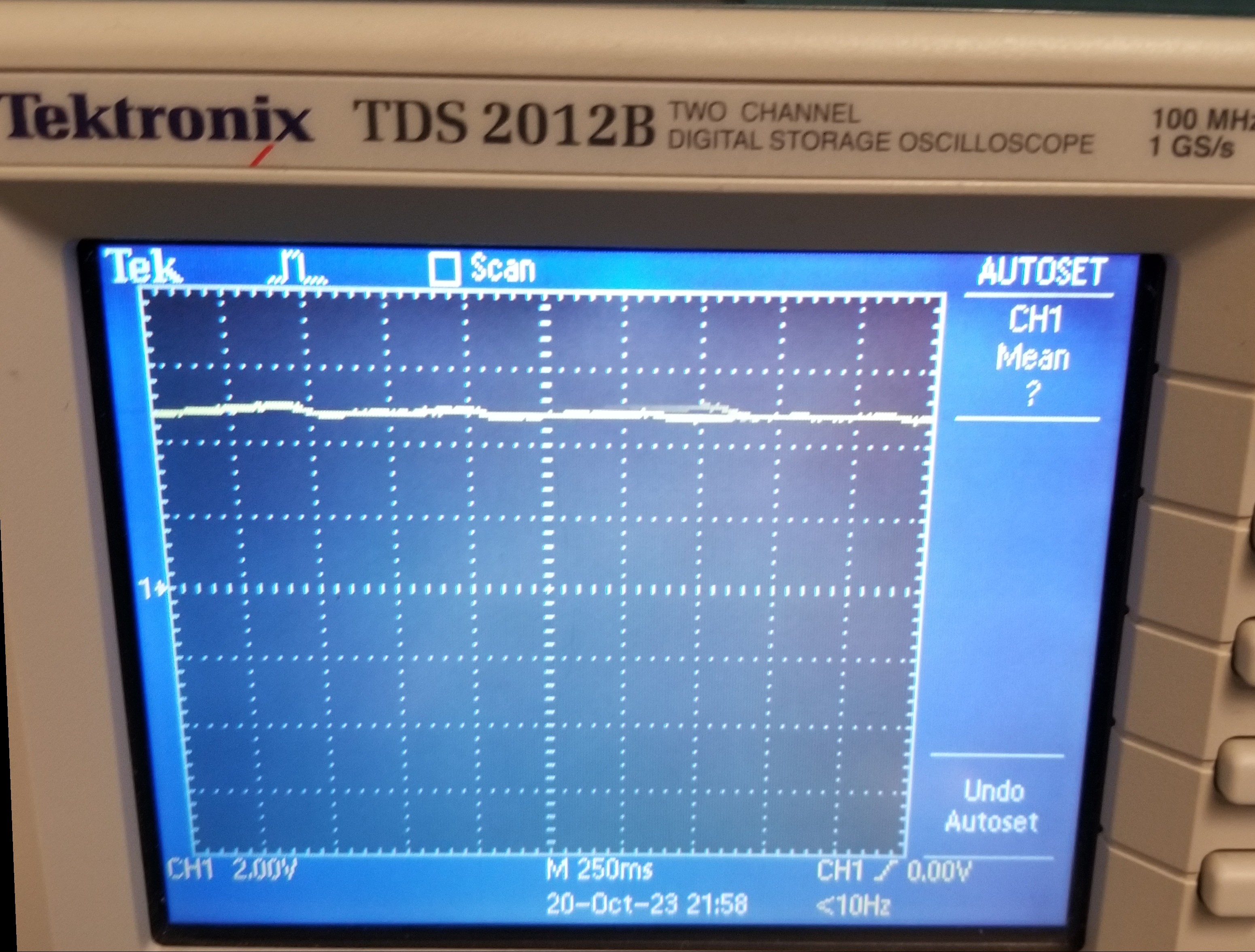
gain for the best performance. Figure 2 shows the initial output for
the transimpedance amplifier circuit.
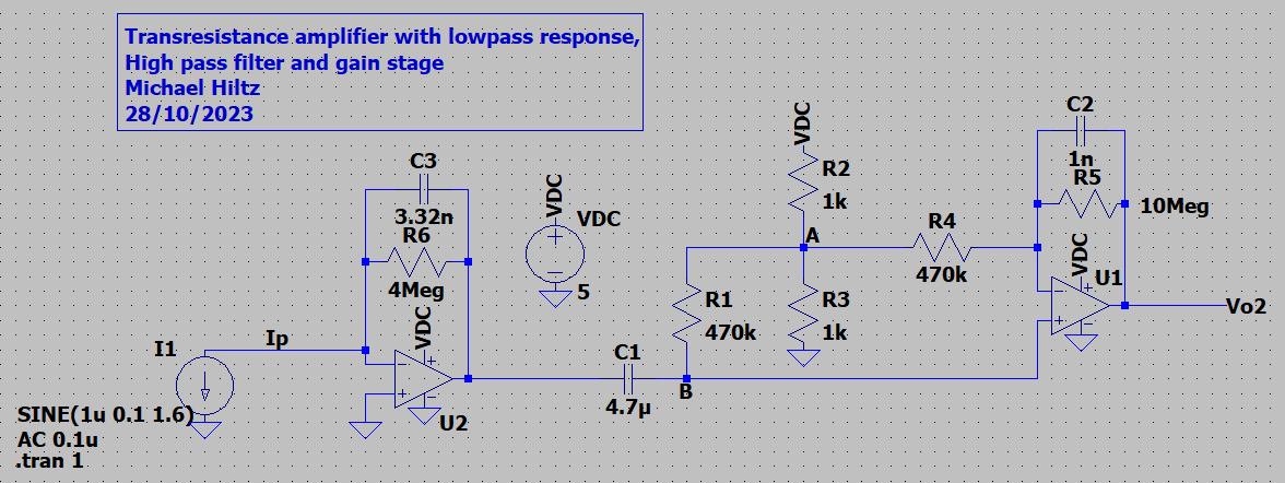
Lab 3: Signal Conditioning
The next step in the project was to condition the signal from the
transimpedance amplifier. This was done by using a bandpass filter to
remove noise from the signal. The bandpass filter was implemented by
adjusting the capacitor in the transimpedance amplifier circuit to
create a low-pass filter, and then adding a high-pass filter after the
amplifier output. The high-pass filter was created using a series
capacitor and resistor to block DC and low-frequency noise, while
allowing the desired PPG signal to pass. The resulting signal was much
cleaner and more representative of the actual physiological signal.
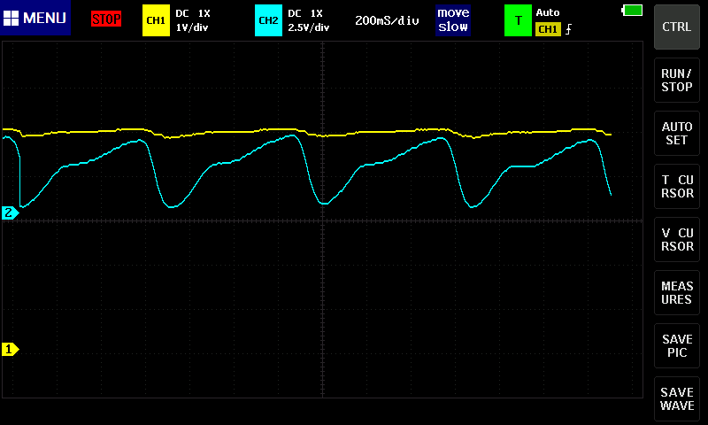
Figure 3 shows the schematic combination of the low-pass and high-pass
filters, with all of the component values, while Figure 4 shows the
output after signal conditioning.
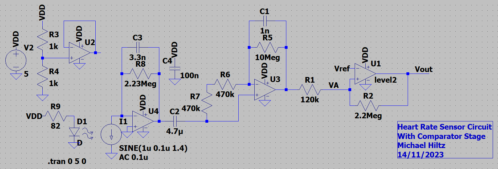
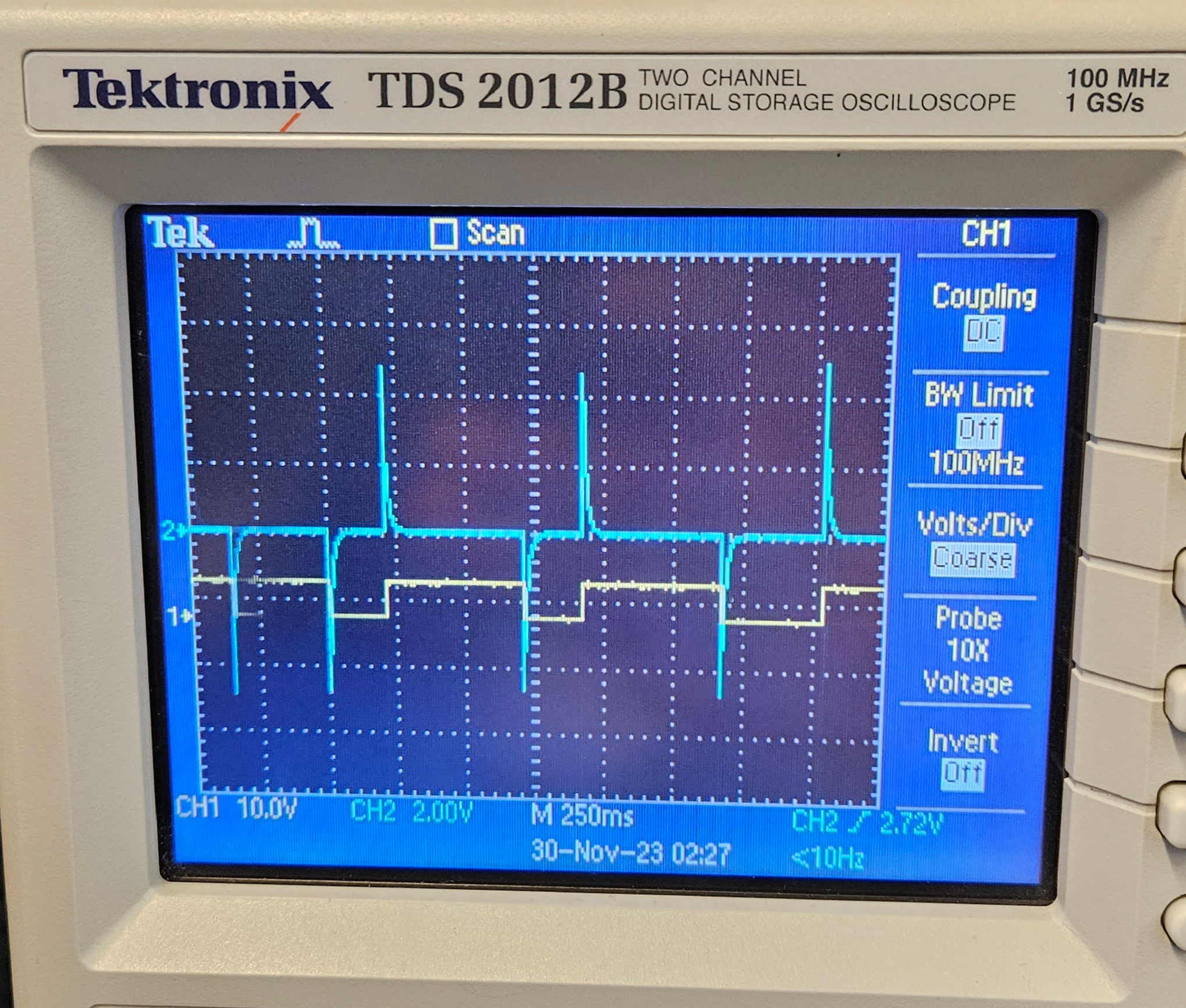
Lab 4: Comparator Design
The second last step in the project was to convert the conditioned
analog signal into a digital switching signal. This was accomplished
by implementing a comparator circuit that could reliably trigger on
each heartbeat. The comparator was designed using an operational
amplifier with positive feedback to create hysteresis, which prevents
false triggering due to noise in the input signal. The circuit
compares the conditioned PPG signal against a 2.5V reference voltage
and switches between high and low output states based on two trip
points. The hysteresis band was carefully calculated to ensure
reliable switching while avoiding false triggers from the dicrotic
notch that appears in PPG signals during cardiac cycles. Figure 5
shows the comparator circuit schematic with component values, while
Figure 6 shows the final digital output signal. The output signal will
be used in the next lab to drive an LED to indicate each heartbeat.

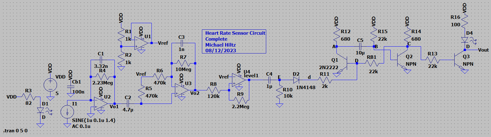
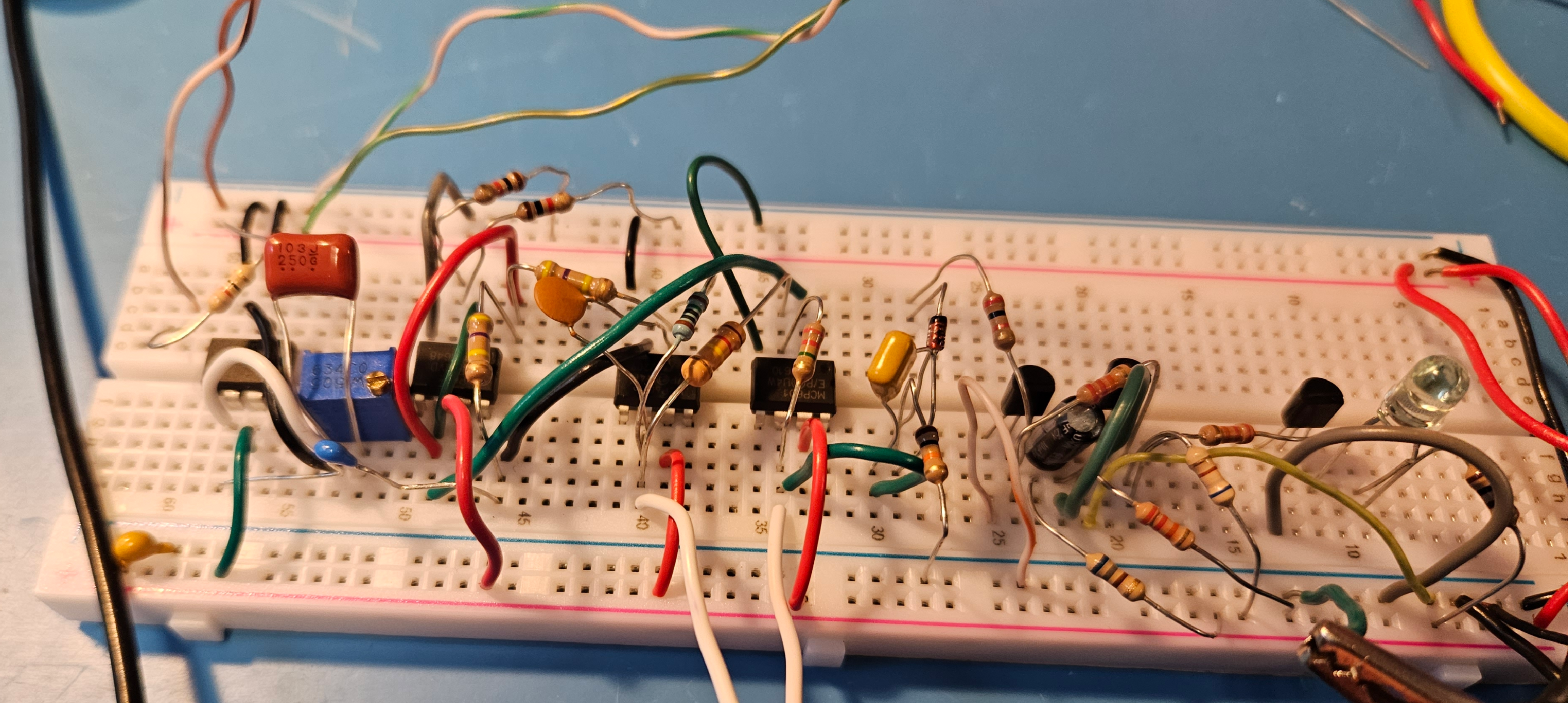
Lab 5: Monostable Multivibrator Circuits
The final step in the project was to create a pulse detection circuit
that would flash an LED each time a heartbeat was detected. This was
accomplished by implementing a three-stage circuit consisting of an
edge detector, a monostable multivibrator, and an LED driver. The edge
detection stage used a differentiator circuit with a coupling
capacitor and input resistor to generate short pulses on the rising
edges of the comparator output, shown in Figure 8. A diode was added
to isolate only the positive-going pulses, ensuring the monostable
circuit would trigger only on heartbeats. The monostable multivibrator
was built using two bipolar transistors configured as a one-shot pulse
generator, with the pulse duration determined by an RC time constant.
For a maximum heart rate of 180 beats per minute, the LED flash
duration was designed to be approximately 200ms to provide clear
visual indication. Figure 7 shows the complete pulse detection circuit
schematic. The final output successfully drives an LED to flash in
sync with each detected heartbeat, providing a simple and effective
visual indicator of the PPG signal. Lastly Figure 9 shows the
completed circuit built on a breadboard.
Reflection
This project provided valuable hands-on experience with analog circuit design and signal processing. By developing the circuit section by section, I gained a deeper understanding of how each type of circuit - amplification, filtering, comparison, and pulse generation - can be used to manipulate a signal to achieve specific goals. Working through the various stages of the PPG circuit helped me understand the principles behind each component and how they interact with the signal as it propagates through the system. The iterative process of testing and refining each section also highlighted the importance of troubleshooting and problem-solving skills in electronics, while demonstrating how different circuit topologies can be combined to create a complete functional system.